On a day loaded with notable highlights, Synopsys, one of the global leaders in Electronics Design and Automation (EDA) with a presence in over 25 countries, announced plans to establish a design-centered facility in Bhubaneswar.

According to an official press release, this facility, which will gradually expand to 300 chip design engineers performing high-tech roles, will include members from top Synopsys teams such as Hardware Analytics and Test (HAT) and Hardware Development Group (HDG), including HDG Analog and HDG Design/Verification.
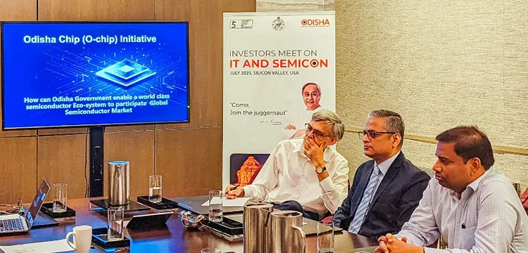
The delegation met with Amit Sanghani, SVP, and Abhijeet Chakraborty, VP, of the company, whose products include tools for logic synthesis and physical design of ICs, simulators for development, and debugging environments, and briefed them on the initiatives the state government is taking to build a resilient semiconductor ecosystem in the state.

The delegation emphasized how the State’s Semiconductor Manufacturing and Fabless Policy, which has been approved by the Cabinet, provides the most generous set of incentives to both fab and fabless units. It also presented information about the planned O-Chip program, which would provide researchers, entrepreneurs, and businesses with design infrastructure as well as training support.
Congratulating the delegation on the efforts of the government, the Synopsys leadership committed its full support to Odisha and later publicly announced the company’s intention to establish a chip design center in the state. The construction of this center will significantly increase Odisha’s semiconductor goals, enhancing the ecosystem and facilitating higher workforce industry preparedness.
The delegation also met with notable industry leaders and researchers in Silicon Valley to provide the finest advisory and mentorship support for the O-Chip program.
With a visionary goal of establishing a next-generation Silicon Valley in Odisha, the O-Chip initiative focuses on several key objectives, including empowering talent and industry expertise, facilitating internship and industry collaborations, forging research partnerships, fueling startup growth, and attracting semiconductor companies. With an initial focus on chips, embedded systems, and AI: Smart Labs, the program seeks collaboration with a diverse network of partners, including semiconductor companies, local and global universities, and a pool of industry experts.
The conversation, which centered on the O-Chip initiative’s mode of operation, operational guidelines creation, and advisory committee establishment, was eagerly participated in by notable industry executives and scholars. They have graciously agreed to serve as advisors and mentors for the effort. Their invaluable leadership and skills will propel the project to new heights, resulting in the active participation of more semiconductor businesses, colleges, and industry experts.

In addition, the delegation attended an event with the Odia diaspora. Members of the delegation addressed the gathering, praising the diaspora for maintaining socio-cultural linkages with the country and for continuing to support Odisha’s growth and prosperity.
More than 900 persons of Odisha origin attended the event, which was organized by the Tourism Department in collaboration with FICCI. The Odia community was hosted by the Consul General and the entire delegation.
The delegation’s visit to Silicon Valley was a huge success, with numerous worldwide IT, electronics, semiconductor, and AI/ML businesses announcing plans to establish operations there. Odisha is seeing a significant increase in investment activity and producing more and more job opportunities as a result of government encouragement and support.
Source:OCN



 Finance